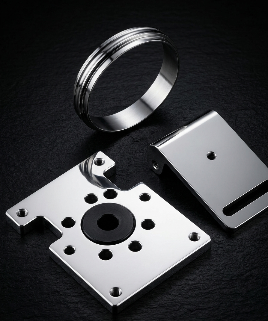
Precision Electroplating Services in Singapore — Built for Performance, Engineered to Last
A precision electroplating guide for Singapore engineers and procurement teams: how plating thickness, adhesion and consistency decide whether a part performs or fails, the standards that matter, and where sub-micron tolerances are non-negotiable.
If you have ever held a hydraulic rod that has survived five years of cyclic load in a saltwater environment, or plugged in a connector that has made a reliable contact ten thousand times without degrading, there is a good chance electroplating is part of why it still works. Electroplating is one of those industrial processes that sits quietly behind almost everything that performs well under pressure. Most people outside the trade do not think about it until something fails, and by then the cost is already far larger than the plating job itself. This guide explains what precision electroplating really involves, why thickness, adhesion and consistency decide whether a part performs or fails, and how engineers and procurement teams in Singapore can specify it with confidence.
What Is Electroplating — And Why Precision Is Everything
Electroplating is the controlled deposition of a metal coating onto a component to give it a property the base metal does not have on its own: corrosion resistance, wear resistance, electrical conductivity, solderability, surface hardness or simply a stable, repeatable finish. The coating is only a few microns thick, yet it carries the entire burden of performance at the surface, which is exactly where parts meet load, friction, chemistry and contact.
That is why precision matters so much. A plating specification is not a cosmetic preference; it is an engineering requirement tied to how the part must behave in service. When the deposit is the right metal at the right thickness, properly bonded and consistent from batch to batch, the component does its job for years. When any one of those variables drifts, the part can look perfect and still fail in the field. Precision electroplating is the discipline of removing that uncertainty.
How Electroplating Actually Works
At its core, electroplating is an electrochemical process. A base metal part, your substrate, is submerged in a chemical bath containing dissolved metal ions. An electrical current is passed through the solution, causing those metal ions to migrate and deposit onto the surface of your part, atom by atom, building up a thin, bonded metallic layer.
The deposited metal, whether nickel, chromium, gold, silver, tin or others depending on the application, bonds at a molecular level to the substrate surface. Done correctly, you end up with a coating that is not just sitting on top of the part. It becomes part of it.
What makes electroplating different from painting or spraying is that bond. A sprayed coating relies on mechanical adhesion. An electrodeposited coating relies on metallurgical adhesion, which is far stronger, far more durable and far more consistent under thermal cycling, mechanical stress and chemical exposure. A related family of processes, such as electroless nickel plating, achieves a similar bonded deposit through an auto-catalytic chemical reaction rather than an external current, which is why it coats complex geometries so evenly.
Why Plating Thickness, Adhesion and Consistency Determine Whether Your Part Performs or Fails
This is where most procurement managers and engineers find out, sometimes the hard way, that not all electroplating is equal. Three variables decide the outcome, and all three must be controlled together.
Thickness
Thickness is the most obvious variable. A nickel deposit specified at 25 microns that is actually being delivered at 12 microns on recessed surfaces is not protecting your part. It is giving you the appearance of protection, and there is a significant difference. In aggressive environments such as salt spray, process chemicals or high humidity, an under-thickness deposit can fail in a fraction of the expected service life. A part specified for 500 hours of salt spray resistance under ASTM B117 will not reach that figure if the coating is thin where it matters most, in the corners, bores and threads where current density is lowest and corrosion starts first.
Adhesion
Adhesion is the variable that kills parts in service without warning. A deposit that has not properly bonded to the substrate can look perfect on day one and delaminate under thermal shock, mechanical impact or cyclic stress. The root cause is almost always inadequate pre-treatment: insufficient cleaning, poor activation of the substrate surface, or contamination in the plating bath. You cannot see poor adhesion in a visual inspection. You find it during a cross-hatch or bend adhesion test, or worse, when the part fails in the field. This is why disciplined surface preparation is not a preliminary step to rush through; it is the foundation the whole deposit depends on.
Consistency
Consistency matters more than most people realise, particularly in high-volume OEM and subcontract runs. If your first batch plates to 22 to 28 microns and your third batch plates to 15 to 35 microns, your downstream process is now managing variance instead of output. For components going into electronics assemblies, medical devices or aerospace sub-systems, that kind of run-to-run inconsistency is not just an inconvenience; it is a qualification failure waiting to happen. Stable bath chemistry, current control, temperature management and routine verification are what keep every batch landing inside the same window.
The Industries Where Sub-Micron Precision Is Non-Negotiable
There is a tier of industries where plating tolerance is written into the engineering specification, cross-referenced against MIL-SPEC, IPC or ISO standards, and verified by third-party testing before a single part ships. These are the sectors where we work every day at Active Treatment.
Semiconductor and Electronics Manufacturing
Semiconductor and electronics manufacturing operates at tolerances that make most industrial plating look coarse. Gold plating on PCB edge connectors is typically specified at 0.5 to 1.27 microns of hard gold over a minimum 2.5-micron nickel barrier, tolerances governed by IPC-4552 and verified by X-ray fluorescence (XRF) thickness measurement. Get it wrong and you are looking at contact resistance failures, gold-tin intermetallic growth at solder joints and field returns that trace back to a coating measured in fractions of a micron. The nickel barrier matters as much as the gold: too thin and copper diffuses through; too thick and cost rises with no benefit. Our work for the semiconductor sector combines gold plating with an electroless nickel underlayer for exactly this reason.
Medical Devices and Precision Instruments
Medical devices and precision instruments bring a different set of constraints. Biocompatibility, surface smoothness and absolute coating integrity are non-negotiable. Electroless nickel on surgical instruments and diagnostic equipment components must meet ISO 10993 biocompatibility requirements. Any porosity in the deposit is a contamination risk. Any peeling is a patient safety issue. For the medical sector, the priority is a dense, pore-free, uniform deposit that survives repeated sterilisation cycles without degrading.
Aerospace and Defence Components
Aerospace and defence components are qualified to specifications such as AMS 2404 for electroless nickel and AMS 2460 for hard chrome, which mandate strict process controls, bath chemistry monitoring and documented traceability for every production run. A single non-conforming batch does not just get rejected. It triggers a corrective action process that can ground a supplier qualification for months. For defence hardware, the paperwork is part of the product: traceability and documented embrittlement relief are as important as the deposit itself.
Oil, Gas and Marine Applications
Oil, gas and marine applications put parts into environments that would destroy unprotected metal in weeks. Pump shafts, valve stems and subsea connector bodies operating in H₂S-bearing or chloride-rich environments require corrosion protection that has been validated, not estimated. Salt spray testing to 1,000 hours or beyond under ASTM B117 is not unusual as a baseline requirement here, and high-phosphorus electroless nickel is frequently specified for its near-amorphous, highly corrosion-resistant structure.
Industrial Tooling and Heavy Machinery
Industrial tooling and heavy machinery round out the picture. Here the primary driver is usually wear resistance rather than corrosion protection: hard chrome plating or heat-treated electroless nickel on press tools, forming dies and hydraulic cylinders, where every additional point of deposit hardness translates directly into extended tool life and reduced downtime. For the manufacturing sector, hard chrome also rebuilds worn shafts and rods back to their original dimensions, turning a scrapped component into a repaired one.
The common thread across all of these industries is that the cost of a plating failure is never just the cost of the part. It is the downtime, the investigation, the rework, the qualification re-run and sometimes, in defence, medical and aerospace applications, the regulatory consequence. Getting the plating right the first time is not a premium. It is the baseline expectation when precision is in the brief.
Our Core Electroplating Services in Singapore
Active Treatment offers a broad portfolio of plating and surface treatment processes under one roof, so the right finish can be matched to each part rather than forced to fit a single capability. The four processes below are the ones most often requested by precision customers.
- Electroless nickel plating: An auto-catalytic deposit that follows part geometry almost perfectly, coating bores, blind holes and threads to a uniform thickness. It combines corrosion resistance and hardness, with high-phosphorus grades for aggressive chemistry and heat-treatable grades for wear. See our detailed electroless nickel plating guide.
- Hard chrome plating: A thick, extremely hard chromium deposit for wear resistance, low friction and dimensional restoration of shafts, hydraulic rods, rolls and moulds. Our hard chrome plating guide covers thickness ranges, grinding and embrittlement relief in depth.
- Gold plating: Stable, low-resistance, corrosion-immune surfaces for connectors, contacts, electrodes and RF hardware, typically applied over a nickel barrier and verified by XRF to IPC-4552 thicknesses.
- Aluminium anodizing: A dense, hard oxide grown into the surface of aluminium parts for wear and corrosion resistance, available in decorative and Type III hard-anodized finishes for tooling and chamber hardware.
Choosing the Right Plating Process
The right process depends on the substrate, the dominant failure mode you are designing against, the operating environment and the dimensional requirement. The table below summarises how the most common precision finishes compare. All values are typical industry ranges and should be confirmed for your specific parts.
| Process | Typical substrates | Main strength | Best suited to |
|---|---|---|---|
| Electroless nickel | Steel, stainless, aluminium, copper alloys | Very uniform coverage plus corrosion and wear resistance | Complex shapes, bores, threads, fluid-path parts |
| Hard chrome | Steel, stainless, cast iron | Extreme hardness and dimensional build-up | Heavy sliding wear, rebuilding worn shafts and rods |
| Gold plating | Copper alloys, nickel-plated parts | Low, stable contact resistance and corrosion immunity | Connectors, contacts, electrodes, RF hardware |
| Aluminium anodizing | Aluminium alloys only | Hard, integral oxide for wear and corrosion | Lightweight tooling, fixtures, chamber parts |
In practice the decision usually starts with the substrate, then narrows by whether the part is fighting wear, corrosion, electrical resistance or a combination. When the choice is not obvious, sending a drawing and describing the service conditions is the fastest way to get a clear recommendation.
How We Control Quality and Verify Every Batch
Precision is only real if it is measured. Reliable electroplating depends on disciplined process control and verification rather than assumption. Adhesion is confirmed through proper pre-treatment and, where required, cross-hatch or bend testing. Thickness is checked with calibrated methods appropriate to the part, including X-ray fluorescence for thin precious-metal and barrier layers where sub-micron accuracy is essential.
Corrosion performance is validated by neutral salt spray testing to ASTM B117 against the specified hour rating rather than estimated from appearance. For high-strength steels, post-plating bake for hydrogen embrittlement relief is documented as part of the process record. Bath chemistry, current density and temperature are managed so that deposit thickness and structure repeat from the first part to the last, which is what keeps qualified jobs qualified.
Why Singapore Manufacturers Choose Active Treatment
Active Treatment has provided metal finishing and surface treatment services in Singapore since 2010, supporting semiconductor, electronics, medical, aerospace, oil and gas and precision manufacturing customers. Because we run a wide range of processes in-house, from electroless nickel and hard chrome to gold plating and anodizing, we can recommend the finish that actually fits the application instead of the one a single-process shop happens to offer. That breadth, combined with calibrated inspection and documented traceability, keeps accountability in one place and shortens lead times.
Whether you are qualifying a new component, solving a recurring field failure or restoring worn parts to specification, our team can advise on the right process, thickness and finish, and verify the result against the standard your sector demands. To go deeper on specific applications, see our guides to surface treatment for the semiconductor industry and surface treatment for medical devices.
Get a Quote for Electroplating in Singapore
Frequently Asked Questions
What is electroplating and what is it used for in Singapore?
Electroplating is an electrochemical process that deposits a thin, metallurgically bonded metal layer such as nickel, chromium or gold onto a base part to add corrosion resistance, wear resistance, electrical conductivity or surface hardness. In Singapore it is widely used across semiconductor, electronics, medical, aerospace, oil and gas and precision manufacturing to make components perform reliably in demanding service conditions.
How much does electroplating cost in Singapore?
Electroplating cost depends on the metal deposited, the specified thickness, part size and geometry, the required finish and the production volume, as well as any testing and traceability the application demands. Because every job is different, the most accurate way to price work is to send a drawing or sample and request a quotation, so the process, thickness and inspection can be matched to the part rather than estimated.
What is the difference between electroplating and electroless nickel plating in Singapore?
Conventional electroplating uses an external electric current to deposit metal, which tends to build faster on edges and high points and less in recesses and bores. Electroless nickel plating is an auto-catalytic chemical process that needs no current, so it deposits a very uniform thickness over complex shapes, blind holes and threads. Electroless nickel is usually chosen when even coverage on intricate geometry, combined with corrosion and wear resistance, is the priority.
How thick should hard chrome plating be in Singapore?
Functional hard chrome deposits typically range from about 5 to 50 microns for wear surfaces, while dimensional restoration of worn shafts, rods and moulds can build up 100 to 500 microns or more before grinding back to size. The correct thickness depends on the load, the type of wear, the operating environment and how much grind stock is needed to finish the part to tolerance, so it should be defined against the drawing and application.
What metal finishing services does Active Treatment offer in Singapore?
Active Treatment provides a full range of metal finishing and surface treatment services in Singapore, including electroless nickel plating, hard chrome plating, gold plating, aluminium and hard black anodizing, zinc plating, chromating, passivation, electropolishing, black oxide and sand blasting. This breadth lets us match the right process, thickness and finish to each part and verify the result with calibrated inspection.
Need Help Choosing the Right Surface Treatment?
Not sure which surface treatment your spare parts need?
Active Treatment Pte Ltd has more than 15 years of experience helping manufacturers, precision engineering firms, semiconductor companies, medical device suppliers and industrial businesses improve corrosion resistance, wear resistance and component lifespan.
Whether you require anodizing, electroless nickel plating, zinc plating, hard chrome plating, electropolishing or another industrial surface treatment, our Singapore engineering team can review your specifications and recommend the most suitable process.
Send your drawings, part specifications or project requirements for a technical consultation.
Email activetreatment88@yahoo.com.sg or phone +65 6352 9846.
Request Technical Consultation · Request Quotation · View Surface Treatment Services
Recommended Services
- Electroless Nickel Plating — Auto-catalytic nickel-phosphorus plating delivering perfectly uniform thickness on complex geometries, blind holes and threads — with medium- and high-phosphorus grades for hardness or 1,000+ hours of corrosion resistance.
- Hard Chrome Plating — Thick industrial hard chrome (5–500+ µm, HV 900–1100) for wear resistance, low friction, and dimensional restoration of hydraulic cylinders, piston rods, and tooling.
- Gold Plating — Precision gold electroplating delivering superior electrical conductivity, permanent corrosion protection, and excellent solderability for connectors, semiconductor contacts, and medical devices.
- Aluminium Anodizing — Electrochemical process that converts the metal surface into a decorative, durable, corrosion-resistant anodic oxide finish. Available in a wide spectrum of colours.