Surface Treatment for the Semiconductor Industry in Singapore
How surface treatment supports semiconductor manufacturing in Singapore, from low-particle electroless nickel and hard-anodized chambers to gold-plated RF contacts and electropolished stainless steel for ultra-clean, plasma-resistant parts.
Singapore sits at the heart of the global semiconductor supply chain, hosting wafer fabs, advanced packaging operations, equipment makers and a deep ecosystem of precision engineering suppliers. The parts that go into this industry, from vacuum chamber walls and electrostatic chucks to RF electrodes, gas manifolds and handling fixtures, live in one of the most demanding environments in manufacturing. They are exposed to high vacuum, aggressive plasmas, corrosive process gases, repeated thermal cycling and relentless cleanliness expectations. In this setting, surface treatment is not a cosmetic afterthought; it is a functional layer that determines whether a component contaminates the wafer or protects it, whether it lasts one campaign or many, and whether a tool meets its particle and yield targets.
This guide explains how surface finishing supports semiconductor manufacturing, the requirements unique to this sector, and which processes are typically specified for different part types. Active Treatment Pte Ltd has worked with precision engineering customers in Singapore since 2010, and this article reflects practical, industry-standard guidance for engineers and buyers serving the semiconductor industry. For a broader view of finishing for tight-tolerance parts, our pillar article on surface treatment for precision engineering parts is a useful companion read.
What Makes Semiconductor Surface Treatment Different
Most industrial finishing aims to protect parts from corrosion and wear. Semiconductor finishing has to do that while also obeying a stricter set of rules. The wafer is the product, and anything the wafer touches, or anything shedding into the chamber, can become a defect. That changes the priorities completely. A finish that performs beautifully on an automotive bracket may be entirely unsuitable for a plasma etch chamber because it generates particles, outgasses, or reacts with process chemistry.
Several requirements recur across the sector:
- Low particle generation. Coatings must adhere strongly and resist flaking, spalling and erosion so they do not shed particulate into the process.
- High purity and low contamination. Finishes should avoid mobile ions and trace metals that can diffuse onto the wafer. Process chemistry, rinsing and cleanliness control all matter.
- Chemical and plasma resistance. Parts face fluorine, chlorine and oxygen-based plasmas, acids and solvents. The finish must withstand the specific chemistry it sees.
- Vacuum compatibility and low outgassing. Porous or oily surfaces release gas under vacuum, slowing pump-down and adding contamination. Smooth, sealed or dense surfaces help.
- Controlled electrical behaviour. Some parts must conduct reliably; others must insulate. The finish is chosen to deliver the right resistivity or contact resistance.
- Dimensional stability and cleanability. Tight tolerances must survive the coating, and the surface must be easy to clean between campaigns.
Because no single finish satisfies every requirement, the right answer depends on the base material, the part geometry and the exact zone of the tool the component serves. Specifying finishing well means matching the process to the function.
Hard Anodizing for Aluminium Chamber Components
Aluminium is the dominant structural material in semiconductor equipment because it is light, machinable, thermally conductive and easy to fabricate into large chambers, lids and brackets. Bare aluminium, however, is soft and reacts readily with process chemistry. Anodizing solves this by electrochemically converting the surface into a hard, integral layer of aluminium oxide.
How anodizing works
In anodizing, the aluminium part is made the anode in an acid electrolyte and a controlled current grows an oxide layer outward from the metal. Standard (Type II) anodizing produces a thinner decorative and corrosion-resistant film, while hard anodizing (Type III) grows a thicker, denser layer that is significantly harder and more wear resistant. Because the oxide is grown from the substrate rather than deposited on top, adhesion is excellent, which directly supports the low-particle goal. Our aluminium anodizing service covers the full range, and the heavier-duty hard black anodizing finish is frequently specified for chamber and fixture hardware.
Why it suits semiconductor parts
A well-controlled hard anodic layer offers wear resistance for moving and frequently handled parts, electrical insulation where needed, and resistance to many of the chemistries used in deposition and etch. For chamber-grade work, attention to the alloy, the cleanliness of the process and the sealing step is critical, because the porous structure of fresh anodize can otherwise trap moisture and contaminants. Sealing surfaces, o-ring grooves, threaded holes and mating faces are usually masked or post-machined to protect tolerances and vacuum integrity. We cover the metallurgy in more depth in our hard black anodizing guide.
It is worth being realistic about limits. Anodizing only works on aluminium, it cannot coat internal bores it cannot reach uniformly, and very harsh fluorine plasmas can still attack standard anodic layers over time. For the most aggressive zones, equipment makers often turn to specialised plasma-resistant ceramic coatings that sit outside conventional wet finishing. Where anodizing is appropriate, though, it remains the practical, cost-effective backbone of aluminium chamber finishing.
Electroless Nickel for Complex Geometries and Fixtures
Electroless nickel plating deposits a nickel-phosphorus alloy through an autocatalytic chemical reaction rather than an external current. That single difference gives it a defining advantage for semiconductor work: the coating builds up to the same thickness on every surface the solution touches, including the insides of bores, blind holes, threads and intricate manifolds where electroplating would deposit unevenly.
Key properties
Electroless nickel offers uniform, conformal coverage, good corrosion resistance, useful hardness that can be enhanced by heat treatment, and a generally smooth as-plated surface. The phosphorus content can be tuned: higher-phosphorus deposits give better corrosion resistance and are largely non-magnetic, which can matter where magnetic interference is a concern, while lower-phosphorus deposits favour hardness. It also plates well onto both steels and aluminium, making it a versatile choice across mixed-material assemblies. Our electroless nickel plating service and the dedicated electroless nickel plating guide go into the chemistry and specification details.
Where it is used
Typical applications include gas and fluid-handling fixtures, manifolds, baseplates, tooling, jigs and handling components that need even protection on complex shapes. Because the coating is uniform, it preserves the geometry of precision parts well, and its corrosion resistance protects steel components from humidity and process exposure. For parts that combine internal passages with external sealing faces, electroless nickel often succeeds where line-of-sight processes struggle. When electrical contact or enhanced surface properties are required on top, nickel also serves as an excellent base layer for subsequent gold plating.
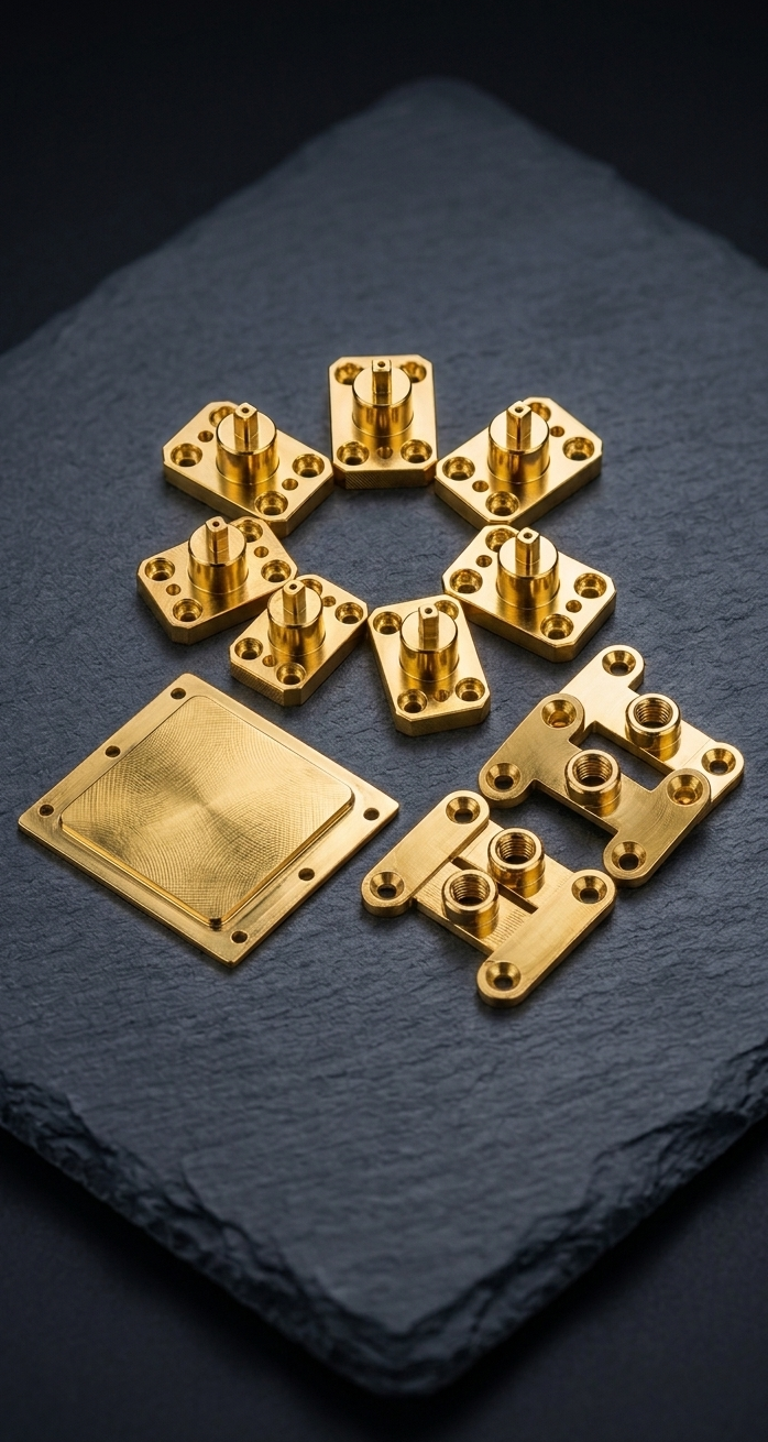
Gold Plating for Contacts, Electrodes and RF Hardware
Where electrical performance is the priority, gold is hard to beat. It combines high electrical conductivity with outstanding corrosion and tarnish resistance, so the contact resistance of a gold surface stays low and stable over time. In semiconductor tools this matters for connectors, electrical feedthroughs, electrodes and RF hardware, where even small, drifting contact resistance can degrade signal integrity, power delivery or measurement accuracy.
How gold is applied
Gold is almost always plated over an underlying barrier layer, typically nickel, which prevents the base metal from diffusing up into the gold and improves hardness and wear life. The gold thickness is chosen to suit the duty: thin flash layers protect and improve solderability or appearance, while thicker deposits are specified for wear at separable contacts and demanding RF surfaces. Hard gold alloys are used where mechanical durability is needed; softer, higher-purity gold is favoured where conductivity and bondability dominate. Our gold plating service supports these requirements with appropriate underplate strategies.
Specifying gold sensibly
Gold is expensive, so good specification means putting it only where it earns its place. Selective or masked plating concentrates the gold on functional contact zones rather than the whole part, controlling cost without compromising performance. Engineers should define the contact area, required thickness, underplate, and any wear or mating-cycle expectations so the finisher can recommend the right build. For RF surfaces, surface smoothness and consistent thickness also influence performance at high frequencies, so cleanliness and process control are part of the value.
Electropolishing for Ultra-Clean, Low-Outgassing Surfaces
Electropolishing is, in effect, the reverse of plating. The part is made the anode in a specialised electrolyte and a controlled current removes a thin layer of metal, preferentially dissolving the microscopic peaks on the surface. The result on stainless steel is a bright, ultra-smooth, deburred surface with a much lower effective roughness than mechanical polishing alone can achieve.
Why it matters for high-purity work
A smoother surface has less area for particles, moisture and contaminants to cling to, which makes parts dramatically easier to clean and faster to pump down under vacuum. That directly supports the low-outgassing, low-contamination goals of semiconductor and high-purity gas systems. Electropolishing also preferentially removes free iron and inclusions and enriches the chromium-rich passive film on stainless steel, improving corrosion resistance, an effect that overlaps with chemical passivation but goes further by also improving surface finish. Our electropolishing service is detailed alongside our electropolishing stainless steel guide.
Typical applications
Electropolishing is widely specified for high-purity gas lines, fittings, valves, fluid-handling components, vacuum hardware and stainless fixtures where cleanability and corrosion resistance are critical. It is best suited to stainless steels and some other alloys; it is not a coating, so it does not add thickness or build up worn dimensions. Because it removes material, designers should account for the small dimensional change on tightly toleranced features and specify the required surface finish clearly.
Matching the Requirement to the Right Finish
Selecting a finish is a process of mapping the dominant requirement of each component to the treatment that delivers it best. The table below summarises common semiconductor finishing decisions. Treat it as a starting point for discussion rather than a rigid rule, because alloy, geometry and the exact process environment always influence the final recommendation.
| Primary requirement | Typical part examples | Recommended finish | Why it fits |
|---|---|---|---|
| Wear and chemical resistance on aluminium chambers | Chamber walls, lids, brackets, fixtures | Hard anodizing (Type III) | Dense, integral oxide with strong adhesion and good chemical and wear resistance |
| Uniform coating on complex shapes and internal passages | Manifolds, fluid fixtures, tooling, baseplates | Electroless nickel | Conformal, even thickness in bores and threads with good corrosion resistance |
| Low, stable electrical and RF contact resistance | Connectors, electrodes, feedthroughs, RF hardware | Gold plating over nickel | High conductivity, corrosion resistance and stable contact behaviour |
| Ultra-clean, low-outgassing, high-purity surfaces | Gas lines, fittings, valves, vacuum hardware | Electropolishing of stainless steel | Very low roughness, easy cleaning and an enriched passive layer |
| Corrosion resistance on stainless without finish change | Brackets, frames, general stainless parts | Passivation | Removes free iron and strengthens the natural chromium oxide film |
In real assemblies, more than one finish often appears on a single tool, and sometimes on a single part through selective masking. A baseplate might be electroless nickel plated for corrosion protection, with gold-plated contact pads for electrical connection. An aluminium fixture might be hard anodized overall with sealing faces masked. The art of finishing lies in combining these processes intelligently.
Designing and Specifying Parts for Finishing
The quality of a finished semiconductor part is decided as much at the drawing stage as in the plating tank. Engineers can prevent most problems by thinking about the finish early and communicating clearly with the finisher.
What to put on the drawing
- Base material and temper. The alloy strongly affects how it anodizes, plates or electropolishes, so state it precisely.
- Finish callout and class. Name the process and any thickness, class or specification you require, rather than leaving it to interpretation.
- Critical dimensions and tolerances. Identify features that must not grow or shrink so they can be masked or post-machined.
- Masking requirements. Call out sealing surfaces, o-ring grooves, threads, bores and electrical contact zones that need protection or selective plating.
- Cleanliness and compliance. State any cleanliness, packaging, RoHS or documentation requirements so the finisher can plan handling and inspection.
Design details that help
Avoid blind pockets and crevices that trap solution and are hard to rinse. Provide drainage and process holes where possible. Remember that plating adds thickness while electropolishing removes it, and that sharp edges build up extra deposit in plating but round off in electropolishing. Sharing the application context, what the part does and what environment it sees, often unlocks a better recommendation than a bare finish code alone. A short conversation before fabrication usually saves rework later.
Cleanliness, Quality and Inspection
For semiconductor parts, what happens after finishing is as important as the coating itself. A perfectly applied finish can still fail if the part is handled carelessly, rinsed poorly or packaged in a way that introduces contamination. Reputable finishers control rinsing, drying, handling and packaging to keep parts clean through to delivery.
Typical quality checks include coating thickness measurement, adhesion verification, visual inspection for defects, and confirmation of masked and critical dimensions. Depending on the finish, additional checks may cover corrosion resistance, surface roughness for electropolished parts, or contact resistance for plated electrical surfaces. The aim is consistency: a finish that performs the same way on every part, every batch, so that tool builders and fabs can rely on it. Documentation and traceability give engineers confidence that what was specified is what was delivered.
It is also good practice to validate a new finish or supplier on representative parts before committing to volume. A first-article approach, where initial parts are inspected thoroughly against the specification, catches misunderstandings early and builds a stable, repeatable process for ongoing production.
Beyond Semiconductors: A Shared Finishing Toolkit
The processes that serve semiconductor manufacturing also underpin other demanding sectors, which is one reason a capable general finisher can support so many applications. Electroless nickel, anodizing and electropolishing are equally relevant to medical device and defence work, where cleanliness, corrosion resistance and reliability are paramount. The same disciplines around masking, dimensional control and inspection carry across industries, even though the specific chemistries and standards differ. Engineers moving between sectors will find the underlying finishing logic familiar.
This cross-industry experience is valuable because it means a finisher has seen a wide range of geometries, materials and failure modes. Lessons learned protecting precision parts in one field often translate directly into better outcomes in another, and a broad in-house process range allows several finishes to be combined on one assembly without juggling multiple suppliers.
Conclusion: Finishing as a Yield Enabler
In semiconductor manufacturing, surface treatment is a quiet but decisive contributor to yield. Hard anodizing protects aluminium chambers and fixtures; electroless nickel delivers uniform protection on complex geometries; gold plating secures stable electrical and RF performance; and electropolishing produces the ultra-clean, low-outgassing surfaces that high-purity systems demand. Chosen well and applied with proper masking, cleanliness and inspection, these finishes help tools meet their particle, corrosion and performance targets campaign after campaign. Chosen poorly, the finish becomes the contaminant. The difference comes down to matching the process to the function and controlling the details.
Frequently Asked Questions
Why is surface treatment so important for semiconductor parts?
Semiconductor tools process wafers in vacuum, plasma and corrosive chemistries where any particle, outgassing source or corrosion product can ruin yield. Surface treatment gives parts the cleanliness, chemical and plasma resistance, controlled conductivity and dimensional stability needed to survive that environment and avoid contaminating the wafer.
Which finish is best for aluminium vacuum chamber components?
Hard anodizing (Type III) is the workhorse finish for aluminium chamber walls, lids and fixtures. It converts the surface into a dense, hard aluminium oxide layer that resists wear, many process chemistries and plasma erosion. For tighter contamination control, sealing and proper masking of sealing surfaces and threads are essential.
When should electroless nickel be specified instead of anodizing?
Choose electroless nickel when you need a uniform, conformal coating on complex geometries, on steels and aluminium alike, with good corrosion resistance and solderability. Its even thickness in bores, blind holes and threads makes it ideal for fixtures, manifolds and fluid-handling parts where anodizing cannot reach internal surfaces.
Why is gold plating used on RF and electrical contacts?
Gold offers very low and stable contact resistance, excellent corrosion resistance and high conductivity, so it is used on connectors, electrodes and RF hardware where signal integrity matters. It is usually plated over a nickel barrier layer to prevent diffusion and improve wear, with thickness chosen to balance performance and cost.
How does electropolishing help in semiconductor and vacuum applications?
Electropolishing removes a thin layer of stainless steel to leave an ultra-smooth, low-roughness surface that is easier to clean, less prone to trapping particles and outgasses less. It also enriches the chromium-rich passive layer, improving corrosion resistance for gas lines, fittings and high-purity fluid components.
What should I send a finisher when requesting a quote in Singapore?
Provide drawings with the finish callout, base material and temper, the affected process environment, required thickness or class, masking and critical dimensions, and any cleanliness or RoHS requirements. Sharing the application context lets the finisher recommend the right process, masking strategy and inspection plan for your parts.
Need Help Choosing the Right Surface Treatment?
Not sure which surface treatment your spare parts need?
Active Treatment Pte Ltd has more than 15 years of experience helping manufacturers, precision engineering firms, semiconductor companies, medical device suppliers and industrial businesses improve corrosion resistance, wear resistance and component lifespan.
Whether you require anodizing, electroless nickel plating, zinc plating, hard chrome plating, electropolishing or another industrial surface treatment, our Singapore engineering team can review your specifications and recommend the most suitable process.
Send your drawings, part specifications or project requirements for a technical consultation.
Email activetreatment88@yahoo.com.sg or phone +65 6352 9846.
Request Technical Consultation · Request Quotation · View Surface Treatment Services
Recommended Services
- Electroless Nickel Plating — Auto-catalytic nickel-phosphorus plating delivering perfectly uniform thickness on complex geometries, blind holes and threads — with medium- and high-phosphorus grades for hardness or 1,000+ hours of corrosion resistance.
- Gold Plating — Precision gold electroplating delivering superior electrical conductivity, permanent corrosion protection, and excellent solderability for connectors, semiconductor contacts, and medical devices.
- Aluminium Anodizing — Electrochemical process that converts the metal surface into a decorative, durable, corrosion-resistant anodic oxide finish. Available in a wide spectrum of colours.
- Hard Black Anodizing — Military-grade Type III hard anodizing producing an exceptionally dense, wear-resistant oxide layer ideal for high-stress aerospace, defence, and semiconductor components.